
An Introduction to MBE Growth
Introduction
Basic Description of MBE
Surface Preparation
Growth Rate Calibration
-BEP
-RHEED Intensity Oscillations
-Surface Normal Reflectivity Oscillations
Epitaxial Growth of AlGaAs
Epitaxial Growth of InGaAlAs on InP
Bibliography
1. Introduction
Molecular beam epitaxy (MBE) was developed in the early 1970s as a means of growing high-purity epitaxial layers of compound semiconductors[1,2]. Since that time it has evolved into a popular technique for growing III-V compound semiconductors as well as several other materials. MBE can produce high-quality layers with very abrupt interfaces and good control of thickness, doping, and composition. Because of the high degree of control possible with MBE, it is a valuable tool in the development of sophisticated electronic and optoelectronic devices. In this chapter we discuss MBE growth of semiconductor layers necessary for resonant-cavity photodetectors.
2. Basic Description of MBE
In MBE, the constituent elements of a semiconductor in the form of 'molecular beams' are deposited onto a heated crystalline substrate to form thin epitaxial layers. The 'molecular beams' are typically from thermally evaporated elemental sources, but other sources include metal-organic group III precursors (MOMBE), gaseous group V hydride or organic precursors (gas-source MBE), or some combination (chemical beam epitaxy or CBE). To obtain high-purity layers, it is critical that the material sources be extremely pure and that the entire process be done in an ultra-high vacuum environment. Another important feature is that growth rates are typically on the order of a few Å/s and the beams can be shuttered in a fraction of a second, allowing for nearly atomically abrupt transitions from one material to another.
The Varian Gen II MBE system at the University of Texas at Austin consists of three main vacuum chambers: a growth chamber, a buffer chamber, and a load lock. The load lock is used to bring samples into and out of the vacuum environment while maintaining the vacuum integrity of the other chambers. The buffer chamber is used for preparation and storage of samples, but other systems have buffer chambers equipped for material characterization as well. The buffer chamber on the UT MBE system also acts as a transition tube to allow samples to be transferred under vacuum to two different Varian Gen II growth chambers, which are nearly identical except that one is set up to grow phosphorus containing III-V compound semiconductors and the other is for arsenic-based compounds. The As-based growth chamber is the one that is used primarily for the work reported here. The growth chamber of a generic MBE system and several of its subsystems are illustrated in Fig. 2.1.
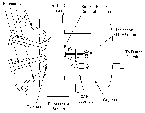
The material sources, or effusions cells, are independently heated until the desired material flux is achieved. Changes in the temperature of a cell as small as 0.5ºC can lead to flux changes on the order of one percent. To control thicknesses to about 1%, highly stable control loops with Tungsten-Rhenium thermocouples and proportion, integral, and derivative (PID) controllers are used as well as a chilled panel separating the cells to prevent thermal crosstalk. Computer controlled shutters are positioned in front of each of the effusion cells to be able to shutter the flux reaching the sample within a fraction of a second. Since shutters in front of the effusion cells reflect some of the power back into the cell, opening the shutters is known to cause flux transients on the order of a few percent with a time constant of several minutes [3,4]. These transients are difficult to measure and depend on cell and system-specific factors such as the shutter type and location, heater element design, and thermocouple placement. The sources in the Gen II system are located approximately 10 cm from the sample in the growth position. In production systems, which are designed for larger wafers and greater uniformity, this distance is larger.
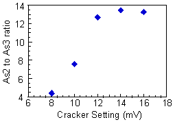
The sources in the University of Texas Gen II system are designed specifically to grow GaAs and other arsenic containing compound semiconductors. The system contains cells for As, Ga, Al, In, Be (p-doping), and Si (n-doping). Because much more arsenic is used than the other materials, the source is more massive and it takes several hours for the As source temperature to stabilize. For that reason, the arsenic source used in our system is a valved cracker[5], in which the flux from a heated As ingot is controlled with a valve. After passing through the valve, the As flux moves through a cracking tube which converts the molecular species from As4 to As2. One of the primary reasons for using As2 instead of As4, is to reduce the consumption of As, since As2 incorporates more efficiently into GaAs. It has also been suggested that using As2 should result in better crystal growth since the incorporation mechanism is simpler than for As4[6]. In order to determine the optimum cracking tube temperature, the mass spectra are recorded for As2 and As3. As4 cannot be measured directly because it is beyond the mass range of the mass spectrometer. The optimum cracking setpoint is chosen to be the temperature at which the As2 to As3 ratio no longer increases with increasing temperature. The data in Fig. 2.2 shows that a setpoint of 14 mV (~800ºC) is a good choice. On an earlier cracker design which used
One of the most useful tools for in-situ monitoring of the growth is reflection high-energy electron diffraction (RHEED). It can be used to calibrate growth rates, observe removal of oxides from the surface, calibrate the substrate temperature, monitor the arrangement of the surface atoms, determine the proper arsenic overpressure, give feedback on surface morphology, and provide information about growth kinetics. The layout of the RHEED system is shown in figure 2.1. The RHEED gun emits ~10KeV electrons which strike the surface at a shallow angle (~0.5-2 degrees), making it a sensitive probe of the semiconductor surface. Electrons reflect from the surface and strike a phosphor screen forming a pattern consisting of a specular reflection and a diffraction pattern which is indicative of the surface crystallography. A camera monitors the screen and can record instantaneous pictures or measure the intensity of a given pixel as a function of time.
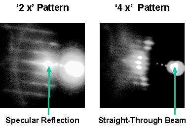
At typical growth temperatures, the surface atoms of an As terminated (100) GaAs layer rearrange themselves into a what is called a '(2x4)' (pronounced 'two by four') reconstruction. RHEED images with the electron beam pointed along the [011] and [
3. Surface Preparation
A clean surface is an important prerequisite for epitaxial growth, since contaminants from the atmosphere or other sources can easily contaminate a clean GaAs wafer and cause crystal defects or degrade the optical and electrical characteristics of the epitaxial layer. Auger electron spectroscopy was an essential tool for determining wafer cleanliness as MBE was being developed [2], but most GaAs wafer vendors currently supply 'epi-ready' wafers which are pre-cleaned and oxidized in a controlled environment. The oxide forms a protective layer which can be removed inside the growth chamber. The use of such epi-ready wafers has lead to consistent results without the need for elaborate wafer cleaning procedures. To use samples of arbitrary size, wafers pieces are cleaved and then bonded using indium to molybdenum blocks. This handling will result in some dust on the wafer surface that will produce defects, but with proper care, the amount of dust can be reduced. The mounted samples are then put into the load lock and heated for several hours to outgas the samples and blocks before moving them into the buffer chamber. The samples are and outgassed again in the buffer chamber at 450ºC before they are moved into the growth chamber.
After the samples are loaded into the growth chamber and moved to face the sources, the RHEED screen will show a haze which is indicative of the amorphous nature of the protective oxide. The substrate temperature is ramped up, with an arsenic overpressure, until a diffraction pattern appears, showing that the oxide has desorbed on the surface. The temperature of the substrate is monitored using a spring-loaded thermocouple in direct contact with the molybdenum block. The deoxidation temperature according to the thermocouple varies often by ~20ºC between blocks and occasionally oxide desorption is observed at more than 40ºC above the usual thermocouple reading. The deoxidation temperature can be used as a temperature reference since it depends primarily on the surface temperature and does not rely on the quality of the contact between the thermocouple and the block. There are still some uncertainties with this method. The transition from hazy to clear diffraction pattern is subjective, and also depends to some degree on the temperature ramp rate and nature of the initial oxide. We use the deoxidation temperature as a reference point for 600ºC and offset the thermocouple reading accordingly, realizing that although it is not completely accurate, this technique increases the repeatability of the temperature measurements. If the system has a window facing the sample, then an optical pyrometer can be used to gauge the temperature. Recently a window was installed in the UT MBE system, but most of the reported temperature readings are obtained from the thermocouple. With the current setup, in order to get enough signal from the sample for a reliable pyrometer measurement, the substrate temperature must be ~600ºC or higher. After RHEED shows that the oxide is gone, the sample temperature is increased 50ºC for 5-10 minutes to ensure that all traces of the oxide are removed.
4. Growth Rate Calibration
4.1 Beam Equivalent Pressure
Calibration of the growth rate is essential for the proper tuning of resonant-cavity devices. There are several in-situ techniques which can be used in MBE. One way to measure the growth rate is to use the BEP gauge. This measurement is dependent on factors such as the geometry of the system and ionization efficiency of the material being measured, but for a given system and material, the BEP reading is proportional to the flux at the sample surface and hence the growth rate. Unlike other techniques we can use, a BEP measurement does not require that any epitaxial layers be grown. Growing epitaxial layers requires an approximate knowledge of the flux beforehand, so the BEP is particularly useful for effusion cells which are being used for the first time. For the Varian Gen II, a BEP reading in the mid to high 10-7 Torr range gives Ga growth rates of about 1 m m/hour. There are limitations to this technique however. It is not a direct measure of the growth rate, so some other in-situ or ex-situ technique must still be used to relate the BEP to a growth rate. The resolution of the BEP gauge in our Varian Gen II can only measure the rates to a precision of several percent. The biggest difficulty, however, is that while measuring the flux of a group III component, the gauge gets coated, causing a rapid loss of sensitivity in the gauge. The gauge sensitivity will eventually recover if left running under an As overpressure, but the measurement is thus uncertain and potentially time-consuming if repeatability is desired.
4.2 RHEED intensity oscillations
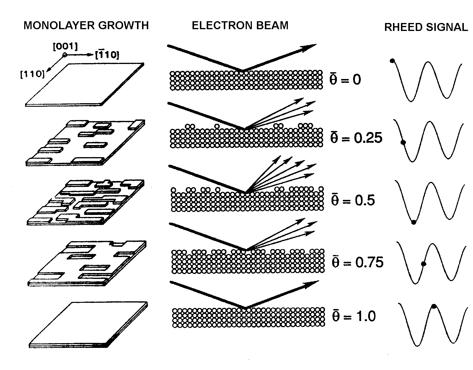
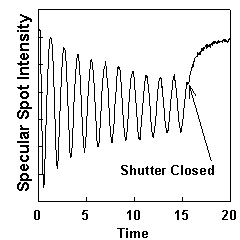
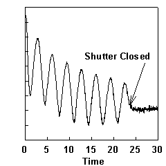
RHEED intensity oscillations can be used as an accurate, quick, direct measure of the growth rates in MBE. When growth is initiated on a smooth GaAs surface, the intensity of the RHEED pattern, especially the specular reflection, starts to oscillate. The oscillation frequency corresponds to the monolayer growth rate [8], where a monolayer (ML) is the thickness of one full layer of Ga and one full layer of As atoms. The oscillations can be explained by a layer by layer growth mode as demonstrated in Fig. 4.1. When a layer starts it is smooth and the specular spot is bright, but as the layer nucleates, islands form on the surface, and the specular spot dims. As the layer finishes, the islands coalesce into a flat layer, and the specular spot intensity increases. The oscillation of the specular spot intensity has been attributed to the oscillating roughness of the layers changing the diffuse scattering [9], but the incident angle dependence of the oscillations [10,11] suggest that interference between electrons scattering from the underlying layer and the partially grown layer contribute to these oscillations. Because the angle of the sample can vary due to wobble in the CAR, the position of the electron gun should be fine-adjusted empirically to get the optimum incident angle.
; (a) (b)
4.3 Normal Incidence Reflectivity Oscillations
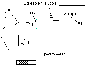
There are other in-situ tools capable of measuring the growth rate accurately including pryometric interferometry[15], optical flux monitoring [16], ellipsometry[17,18], and normal incidence reflectometry [19,20]. In order to try to get more accurate layer thicknesses we have recently implemented a normal incidence reflectometry capability because it is relatively simple and requires little modification to the growth chamber. If there is a port facing the substrate, as there is on Varian Gen II systems, a viewport and a shutter to prevent the viewport from getting coated can be installed. For reflectometry measurements, the shutter needs to be left open for extended periods of time, which will cause the viewport window to get coated unless it is heated to at least 200ºC. If the window gets coated, then heating to about 300ºC for a couple hours is usually sufficient to clean it. These temperatures are too high for a standard viewport, so a special bakeable sapphire or quartz viewport must be used.
A sketch of the optical monitoring setup is shown in Fig. 4.3. Light from a lamp is directed into a fiber. A lens focuses the light and directs the light through the viewport to the sample. The distance from the lens to the sample is about 20 cm, and the spot size is about 1 cm in diameter at the sample. The CAR is aligned so that the reflected light passes back through the viewport and lens, and into a fiber which leads to an optical spectrometer with a detection range of 0.7 m m to 1.1 m m and 512 resolved wavelengths.
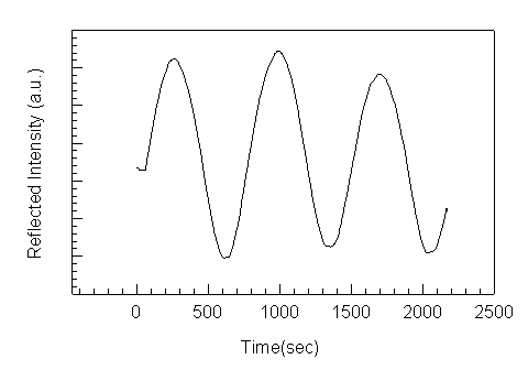
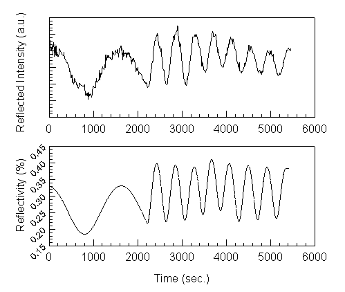
Monitoring the growths real-time is appealing since it can be used to compensate for unexpected flux drifts from the effusion cells, but is more difficult to implement. One problem is that during a growth the sample must be rotated. The CAR wobbles with rotation, which causes the measured signal to fluctuate. The signal fluctuation due to wobble can be much larger than the oscillation magnitude due to reflectivity changes in the sample and can thus wash out the signal. As a test, the reflected intensity at 0.95 m m is measured during growth with rotation of a p-i-n photodiode. The first layer of the structure is a 200 nm thick AlAs layer, followd by a 300 nm thick Al0.3Ga0.7As p-doped layer, a 100 nm graded AlxGa1-xAs layer, a 200 nm thick GaAs absorption layer, another 100 nm graded layer, and an n-doped Al0.3Ga0.7As layer with a 10 nm GaAs cap layer. Figure 4.5 shows the calculated reflectivity and the measured reflected intensity as a function of time. During growth the sample is rotated at 5 r.p.m. The integration time of the spectrometer is set so that one data point is measured every 12 seconds, which is the time for one rotation. When the integration time is not equal to the time for an integral number of rotations, the noise can be larger than the signal, depending on the strenght of the oscillations and the amount of wobble for a particular sampleblock.
There are several important differences in the measured and calculated data in figure 4.5. The magnitude of the oscillations damp for both results, but much more rapidly in the measured data. The damping is due to optical absorption in the layers, which is not adequately modeled in the calculations at 600ºC. The calculated reflectivity is based on growth rates measured by RHEED oscillations on a small calibration sample and the indices of refraction are extrapolated from values in the literature. Considering that RHEED growth rates and optical parameters from the literature result in about a systematic 5% offset between measured and calculated thicknesses at room temperature, it is surprising that the measured and calculated results differ by less than 1% for this sample. Because the layers are graded by adjusting the temperature of the aluminum effusion cell, and because the transient response of the cell is not accurately characterized, there is an additional error in the thickness. It is possible, in this case, that the errors due to growth rate uncertainties and errors in the refractive index offset each other. Regardless, this example shows that reflectometry can be used to monitor a typical sample during growth with rotation and accurately determine if the proper structure is grown.
Consider the case that there is a small error in the thickness of one of the layers in the quarter wave stack. The QWS will then have a phase shift at the desired resonant wavelength and unless corrections are made in the thickness of the cavity, the final structure will be resonant at the wrong wavelength. It is possible to measure the reflectivity of the QWS as a function of wavelength, try to deduce the error, and simulate the structure with an adjusted QWS to determine which wavelength to monitor and at what point to stop the oscillation. Such a procedure is
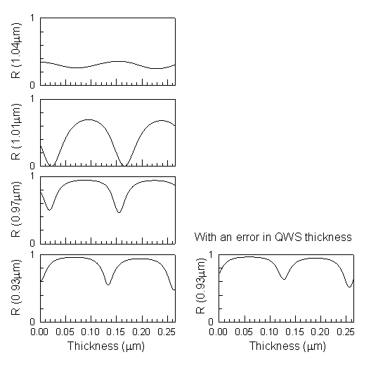
Monitoring the growth of In0.53AlxGa0.47-xAs optical cavities resonant at 1.3 m m or 1.55 m m is more difficult, since the spectrometer is only capable of measuring wavelengths to 1.1 m m. The spectrometer cannot measure wavelengths near the high-reflectivity band of the quarter wave stack, which weakens the measurable oscillation strength and makes it difficult to compensate for optical phase shifts due to errors in the QWS. For alloys with a high Ga fraction, the absorption in the layers at the detectable wavelengths is very strong and the signal will damp quickly, limiting the total thickness that can be monitored. In addition, the sample must be rotated during growth, or the composition will be non-uniform and the layers will not be lattice-matched to the substrate. We have already shown that measuring during rotation is possible, but produces noisier data. Since there are few reports of the temperature dependence of the refractive indices for InGaAlAs, it is necessary to determine these values. If the growth rate from RHEED oscillations is taken to be the actual growth rate, then reflectivity oscillations at 0.9 m m during growth of In0.52Al0.48As reveal an index of refraction of 45±0.1 at ~510ºC. This value is less that the refractive index of 3.5 which is used in the calculations for In0.52Al0.48As for the room temperature refractive index at 0.9 m m, but we have already noted that there is a systematic discrepancy between growth rate determined from the calculated refractive indices and from RHEED oscillations.
5. Epitaxial Growth of AlxGa1-xAs
When molecules arrive at the substrate, they can adsorb, migrate on the surface, interact with other atoms, incorporate into the crystal, or desorb. The primary controllable factors that affect this process are the surface, the temperature of the substrate, and the incident fluxes. At substrate temperatures typically used for growth of GaAs(~580ºC-650ºC) arsenic desorbs from surface of GaAs preferentially, requiring an As overpressure to prevent the surface from becoming Ga rich. It was also noticed early in the development of MBE [21] that the presence of Ga adatoms on a GaAs surface greatly increases the adsorption rate of As2. The sticking coefficients of As species are proportional to the Ga flux and approach 1 for As2 or 0.5 for As4 [6]. The dependence of the As sticking coefficient on the presence of a group III molecule enables the films to grow stoichiometrically over a relatively large range of substrate temperatures and As overpressures.
At temperatures up to ~650ºC, the sticking coefficient of Ga on GaAs is near unity. The sticking coefficient of Al on AlxGa1-xAs is near unity even above 700ºC. With unity sticking, the growth rates of each group III constituent are determined primarily by the temperatures of the effusion cells and it is therefore relatively straightforward to control the growth rates and determine the alloy composition. However, if the substrate temperature during growth exceeds the unity sticking temperature range, then the sticking coefficients of the group III adatoms can depend on the As overpressure, the substrate temperature, and the alloy composition [22,23].
The surface mobility of the group III adatoms plays an important role in the morphology and quality of the layers. If the adatoms are able to diffuse to steps on the surface where they incorporate preferentially, then the growth surface will be nearly layer by layer. The group III adatoms' surface mobility is affected by the group III species, the substrate temperature, the surface on which the adatoms are moving, and the group V overpressure. Higher substrate temperature and lower group V flux both result in higher surface mobility. This tendency would imply that higher substrate temperatures and lower group V fluxes should produce smoother layers as long as the group V flux is sufficient to maintain proper stoichiometry. This improvement in smoothness with increased temperature is supported, for example, by observations of improved mobility in inverted HEMTs grown at higher temperatures [24]. When growing GaAs, there is a large window for which there is both unity sticking and sufficient mobility. When growing ternary or quaternary compounds, the window of good growth conditions becomes significantly smaller because of the differences in the relative bond strengths of the different group III adatoms. Surface mobility is not the only factor important for good morphology, however. The growth of AlAs at 600ºC is smooth and shows strong RHEED oscillations, as seen in Fig. 4.2 (b), even though the mobility of the Al adatoms is significantly less than the mobility of the Ga adatoms. Despite smooth morphology for growth with substrate temperatures of ~600ºC and ~700ºC, high Al content (x>0.4) AlxGa1-xAs layers show increased roughness when grown in the temperature range of 630ºC-690ºC [26]. We generally use a growth temperature of ~600ºC for AlxGa1-xAs, because it results in good material for the entire range of compositions and maintains unity sticking conditions for the group III components. It is also a convenient temperature since it is close to the deoxidation temperature, which is used as a temperature reference.
RHEED can be used to determine the minimum amount of As required to maintain the proper stoichiometry by measuring the incorporation ratio. This measurement starts with a sample at the growth temperature under an As flux, ensuring that the surface is As-terminated. The As shutter is closed and the Ga shutter is opened for a few seconds, causing the surface to become Ga terminated and the RHEED pattern to change. The As shutter is then reopened with the Ga shutter still open and the time required for the surface to recover is recorded. If the RHEED never recovers, then the As flux is too low. If it changes back very quickly then the As pressure is probably too high and the mobility of the group III adatoms will be too low. An incorporation ratee ratio can be expressed as the total time the Ga shutter is open until the surface recovers divided by the time it takes for the surface to recover after the As shutter is reopened or
 . (5.1)
Values of the incorporation ratio of 1.3 to 1.8 typically yield good results for GaAs and AlAs. The As flux can then be measured with the BEP gauge, and in subsequent runs with the same substrate temperature and growth rate, the As flux can quickly be set to the same BEP without needing to remeasure the incorporation ratio. The BEP for 1 ML/s GaAs growth at ~600ºC is typically either 4.5x10⁻⁶ Torr or 6x10⁻⁶ Torr depending on which of two ion gauge filaments is used. The dependence on a small displacement of the filament highlights the fact that BEP measurements are system dependent and that a system independent measurement, such as an incorporation ratio, is a better gauge of the growth conditions.
If a smoother morphology is desired, but the growth temperature can't be increased, there are other ways of improving the smoothness of the layers. Growing the layers slowly allows more time for the adatoms to move on the surface and can thus lead to smoother films at low temperatures [27]. Slow growth rates, however, are impractical for thick layers and will also lead to an increased background impurity concentration. For improved interface smoothness, pausing growth at the interface can be used [28,29], but lengthy pauses can be a problem at critical layers since background impurities will accumulate at the interface during the pause. Because the diffusion length of a group III adatom can be more than an order of magnitude larger when no As overpressure is present, modulating the As and group III fluxes can enhance the adatom mobility during epitaxial growth and has thus been termed migration enhanced epitaxy (MEE) [30]. In addition to MEE, which is often avoided because the rapid shuttering is hard on the effusion cell shutters, the use of substrates that are cut a few degrees off axis has been shown to improve surface morphology [31]. The surface of an off-axis substrates has a higher density of surface steps and thus decreases the distance that adatoms need to diffuse to reach a step edge. Because of the high density of step edges, much of the growth occurs by step propagation, which cannot be monitored by RHEED oscillations. Different crystal orientations have different growth characteristics and are of some interest, but (100) is the predominant substrate orientation for MBE growth of compound semiconductors because it produces good quality epilayers and is free from the antiphase, twinning, and faceting defects present common in epilayers grown on the (111)A, (111)B, and (110) surfaces.
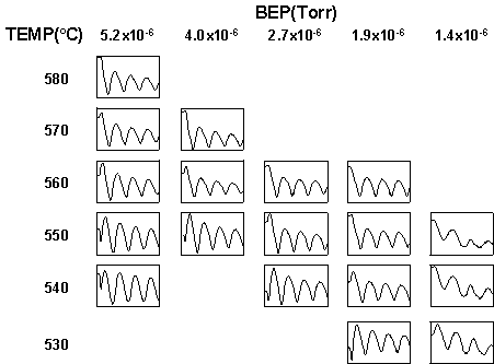
At reduced substrate temperatures and/or increased As overpressures, the surface becomes As-rich and changes to a (2x2) reconstruction. This transition can be used to glean some useful information about the growth conditions. Figure 5.1 shows the start of RHEED specular spot oscillations for a range of As overpressures and temperatures. The specular spot on As-stabilized (2x4) surfaces starts oscillating
6. Growth of InGaAlAs on InP
The discussion in previous section focuses primarily on the growth of AlxGa1-xAs on GaAs, but there is considerable interest in the growth of materials with a smaller bandgap for use in longer wavelength detection. Incorporating In into AlxGa1-xAs will decrease the bandgap, but unlike AlGaAs which is essentially lattice-matched at all alloy compositions, increasing the In content in InGaAlAs increases the lattice constant. If the In content is maintained at about 53% of the group III content, then the material will be lattice-matched to another readily available substrate, InP. The bandgaps available in this lattice-matched quaternary ranges from 1.49 eV for In.52Al.48As to 0.74 eV for In.53Ga.47As, which is a small enough bandgap to detect light at the important wavelengths of 1.3m m and 1.55m m. This section will discuss issues pertaining to the growth of InGaAlAs on InP for optoelectronic applications.
6.1 Surface Preparation
The surface preparation of InP wafers differs from the preparation of GaAs wafers, so this section will discuss the parts of the procedure which are different. InP wafers are also available in epi-ready form, so cleaning procedures before loading samples into the vacuum are not necessary. The outgassing temperature must be kept low, however, since the incongruent sublimation temperature (Tc) of InP is only 360ºC, compared to 650ºC for GaAs[32]. The low Tc is also a problem for deoxidation of the surfaces, since temperatures near 500ºC are needed to remove the oxides. A common method for preventing the InP from decomposing is to use an As overpressure, which has been shown to prevent thermal damage to the substrate even at 500ºC [33]. One concern is that the As will eventually replace the P and result in a strained InAs interfacial layer. There are conflicting reports both that a couple monolayers of InAs are formed during the cleaning process [34] and that only about 5% of the P atoms at the surface will be replaced by As [35] even after a hour at 500ºC. One InP wafer supplier, Crimsatec InPact, suggests that ramping the wafer temperature to 565ºC at 25ºC/min under an As overpressure is best to remove all traces of oxygen on the surface. Careful monitoring of the RHEED image is required to ensure that the temperature does not go too high. Upon transformation from a (2x4) to a (4x2) reconstruction near 565ºC, the sample must be cooled immediately and growth initiated. This technique works well, but we find that the surface transformation occurs at 530ºC-540ºC. Since the UT-Austin MBE machine has two growth chambers connected by a vacuum transfer tube, one of which can supply a phosphorus overpressure, it is more straightforward to remove the InP oxide under a phosphorus overpressure. This enables higher temperatures to ensure that the oxide is completely removed without worries of causing interfacial strain due to the formation of InAsyP1-y layers. After the oxide has been removed, the sample is cooled and transferred under vacuum to the As system for InxGa1-xAs growth.
6.2 Growth rate calibration
Because the layers must be lattice-matched, the growth rates must be calibrated accurately to achieve high quality material. As mentioned before, the BEP gauge can be used for a rough estimate of the flux, but is not easy or reliable because coating the gauge with group III sources quickly decreases the sensitivity of the gauge. RHEED of InGaAs directly on InP surfaces is also a problem initially because the material must be nearly lattice-matched before RHEED oscillations can be measured.
The easiest solution is to precalibrate the Ga, Al and In components on a GaAs substrate first. The Ga and Al calibrations are straightforward, but since InAs is not lattice-matched to GaAs, a more indirect method must be used. Thin layers of InxGa1-xAs with low In concentrations (x<0.25) grow pseudomorphically on GaAs, so the indium component of the growth rate is the growth rate of the InGaAs layer minus the growth rate of the GaAs layer. All of the calibrations must be done under unity sticking conditions, which means that the substrate temperature must be less than 550ºC for the InGaAs layers. In addition, after each InGaAs calibration, a thick GaAs buffer layer must be grown to prevent the relaxation of the layers through the formation of misfit dislocations. If the growth rate of the GaAs is set to 1.2 ML/s, then to keep the In fraction to less than 0.25, the maximum growth rate of In that can be calibrated this way is ~0.4 ML/s. Because of the high growth rate and the high In fraction, the oscillations will be poor and therefore will have a large uncertainty. Higher In growth rates can be set by extrapolating the growth rate vs. effusion cell setpoint to higher rates.
The In rates are uncertain when measured on GaAs, but once the rates are set near the proper ratio for lattice matching, (In/(Ga+Al) = 0.53/0.47), fine-tuning of the In rate can be done on InP substrates to improve the accuracy. Due to the unequal lattice constants, the growth rates for a given material flux on GaAs must first be adjusted to the equivalent growth rates on InP. The conversion relation is
Rate on InP = Rate on GaAs *
 .
(6.1)
.
(6.1)
The lattice constants (a) are listed in table 6.1. The growth rate of InGaAs is measured on an InP calibration sample and the In component of the rate is simply the total growth rate minus the adjusted GaAs growth rate. If the epitaxial layer is near the lattice-matched composition, then the InGaAs RHEED oscillations will be strong and repeatable. Further improvement in the composition accuracy can be obtained by measuring samples with X-ray diffraction, and adjusting the rates accordingly.
The lower bond energy of In introduces constraints on the growth conditions beyond what is required for growth of AlxGa1-xAs. The sticking coefficient for In in InGaAs layers decreases significantly below unity above 525ºC [36,37]. High-quality In0.53Ga0.47As layers and devices are reported with a substrate temperature range of ~450ºC-520ºC [38-41]. The growth of InAlAs has different growth requirements. Disorder due to alloy clustering [42] reduces the window of optimum growth conditions compared to InGaAs. The reported optimum conditions for In.52Al.48As are often contradictory. Some reports say that high-quality In.52Al.48As are achieved at substrate temperatures greater than 550ºC [41] while other report that the morphology of In.52Al.48As layers degrades significantly above 540ºC [42]. Other reports indicate that, due to the large difference in In-As and Al-As bond energies, alloy clustering is a problem[43], and thus it is preferable to use moderate temperatures and high As overpressures. This growth condition reduces the adatom mobility which reduces clustering but still results in smooth morphology. Studies of X-ray linewidths and material mobility suggest an optimum temperature in the range of 525ºC and a relatively high As overpressure of 1.5x10⁻⁵ Torr [44]. To achieve good quality layers of both In.53Ga.47As and In.52Al.48As without the need to adjust the temperature or As overpressure, we use a substrate temperature of ~520ºC and an As overpressure of 1.3x10⁻⁵ Torr, which is about is about 3 times larger than the overpressure used for GaAs growth at 600ºC.
Because effusion cell temperatures drift, especially over the long time needed to grow a resonant cavity and since calibrations are not always accurate, a perfect lattice-match is difficult to achieve. It is therefore important to know how stress affects the quality of the layers. If the lattice mismatch is too great, misfit dislocations will form, but even if misfit dislocations don't form, the strain can influence the crystal growth. Layers grown under a small degree of compressive strain (positive mismatch: D a/a~10-3) have good morphology and electrical characteristics, while samples grown under the same level of tensile strain (negative mismatch) [41,45], show a strong degradation in morphology. The observation of strong, persistent RHEED oscillations for the case of compressive strain [46] is consistent with the morphology observations and implies that the growth proceeds in a layer by layer mode under compressive strain. These observations suggest that if the film deviates from a perfect match, it is better to err on the side of having slightly In-rich films.
7. Mismatched Absorption Layers
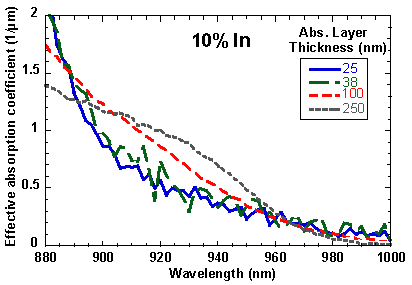
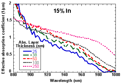
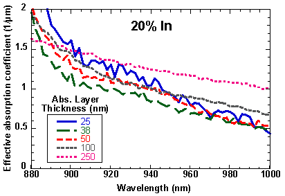
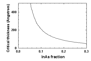
For photodetectors capable of detecting in the range of wavelengths just longer than the absorption cutoff for GaAs, thin InxGa1-xAs layers with low In content (x = 0.1-0.2) can be used as an absorption layer. This approach is often desirable since it takes advantage of the AlxGa1-xAs material system and allows for detection of light in the wavelength range of 0.88 m m to 1 m m. One of the main problems with this approach is that the InGaAs layers are mismatched and growing the layers beyond a critical thickness leads to the formation of misfit dislocations which thread through the epitaxial layers and can cause increased dark current, early breakdown of avalanche photodiodes, and reliability problems. This section examines the use of mismatched InxGa1-xAs layers for use in p-i-n photodetectors and avalanche photodiodes.
To measure the absorption coefficient, three sets of GaAs p-i-n photodiodes with InxGa1-xAs absorption layers (x=0.10, 0.15, and 0.20) are used. Within each set of photodiodes, the thickness of the absorption region ranges from 25 nm, to 250 nm. Thinner layers are not measured, in order to avoid the effects of quantum confinement on the absorption. The external quantum efficiency, h ext is measured by passing white light through a monachromator, focusing it on the sample and measuring the photocurrent, Imeas, for a range of wavelengths. The measured photocurrent is compared to the photocurrent (Istnd.) produced by a calibrated photodiode under identical illumination. Since the standard photodiode is calibrated in terms of the responsivity, Rstnd., with the units of Amperes/Watt, and quantum efficiency is reported in terms of generated electron-hole pairs per incident photon, the external quantum efficiency at a given wavelength can be written as
The external quantum efficiencies are measured from 0.88 m m to 1.0 m m. A reference sample with a GaAs absorption region shows that absorption in the GaAs layers is not substantial at wavelengths longer than 0.88 m m. Since only the InxGa1-xAs layer absorbs light, the effective absorption coefficient, a, for an absorption layer thickness, d, can be extracted from h eff by using the equation
The top surface reflectivity, R, is taken to be 0.3, which is the reflectivity of an air/GaAs interface.
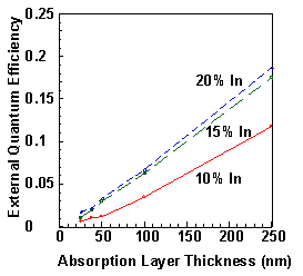
The external quantum efficiency at a wavelength of 940 nm is shown in Fig. 7.1. The quantum efficiency increases as would be expected for increasing absorption layer thickness. To distinguish between the effects of the absorption coefficient, a, which is a material property, and the layer thickness, d, the quantum efficiency results are used to extract a using Eq. 7.2. Figures 7.2-7.4 show the absorption coefficient for the InxGa1-xAs layers with different thicknesses and compositions. In most of the wavelength range of interest, the thickest layers, in fact
8. Bibliography
[1] A. Cho, "Film Deposition by Molecular Beam Techniques," J. Vac. Sci. Tech., Vol. 8, pp.S31-S38, 1971.
[2] A. Cho, J. Arthur, "Molecular Beam Epitaxy," Prog. Solid-State Chem., Vol. 10, pp. 157-192, 1975.
[3] G. Turner, B. Nechay, S. Eglash, "Frequency-Domain Analysis of Time Dependent Reflection High-Energy Electron Diffraction Intensity Data," J. Vac. Sci. Tech. B, Vol. 8, pp. 283-287, 1990.
[4] R. Fernandez, A. Harwitt, D. Kinell, "Accurate Measurements of Transients and Intentional Rates of Change in Molecular Beam Epitaxy Growth Rate Calibrations," J. Vac. Sci. Tech. B, Vol. 12, No. 2 , pp.1023-1025, 1994.
[5] T. Mattord, K. Sadra, A. Srinivasan, A. Tang, T. Block, Y. Shih, D. Neikirk, B. Streetman, "Real-Time Flux Monitoring and Feedback Control of a Valved Arsenic Source," J. Vac. Sci. and Tech. B, Vol. 11, No. 3 , pp. 1050-1052, 1993.
[6] C. T. Foxon, "MBE Growth of GaAs and III-V alloys," J. Vac. Sci. and Tech. B, 1, No. 2 , pp.293-297, 1983.
[7] V. Swaminathan, A. Macrander, Material Aspects of GaAs and InP Based Structures, p. 191, Prentice-Hall, 1991.
[8] J. Harris, B. Joyce, P. Dobson, "Oscillations in the Surface Structure of Sn-Doped GaAs During Growth by MBE," Surf. Sci., Vol. 103, pp.L90-L96, 1981.
[9] J. Neave, B. Joyce, P. Dobson, N. Norton, "Dynamics of Film Growth of GaAs by MBE from RHEED Observations," Appl. Phys. A, Vol. 31, pp.1-8, 1983.
[10] P. Cohen, P. Pukite, J. van Hove, C. Lent, "Reflection High Energy Electron Diffraction Studies of Epitaxial Growth on Semiconductor Surfaces," J. Vac. Sci. Tech. B, Vol. 3, pp. 1251-1258, 1986.
[11] T. Block, K. Eyink, D. Neikirk, B. Streetman, "Diffraction Condition Dependence of RHEED Dampening During MBE Growth," SPIE Proceedings, Epitaxial Growth Processes, Vol. 2140, pp. 10-24, 1994.
[12] M. Ohring, The Material Science of Thin Films, Academic Press, 1992.
[13] J. van der Wagt, J. Harris, "Reflection High Energy Electron Diffraction Intensity Oscillations during Molecular Beam Epitaxy on Rotating Substrates," J. Vac. Sci. Tech. B, Vol. 12, No. 2 pp. 1236-1238, 1994.
[14] G. Petrich, P. Pukite, A. Wowchak, G. Whaley, P. Cohen, A. Arrot, "On the Origin of RHEED Intensity Oscillations," J. Crystal Growth, Vol. 95, pp. 23-27, 1989.
[15] R. Sacks, R. Sieg, S Ringel, "Investigation of the Accuracy of Pyrometric Interferometry in Determining AlxGa1-xAs Growth Rates and Compositions," J. Vac. Sci. Tech. B, Vol. 12, No. 3 , pp.2157-2162, 1996.
[16] P. Pinsukanjana, A. Jackson, J. Tofte, K. Maranowski, S. Campbell, J. English, S. Chalmers, L. Coldren, A. Gossard, "Real-time Simultaneous Optical-Based Flux Monitoring of Al, Ga, and In using Atomic Absorption for Molecular Beam Epitaxy," J. Vac. Sci. Tech. B, Vol. 14, No. 3 , pp.2147-2150, 1996.
[17] W. Gilmore III, D. Aspnes, "Performance Capabilities of Reflectometers and Ellipsometers for Compositional Analysis During AlxGa1-xAs Epitaxy," Appl. Phys. Lett., Vol. 66, No. 13 , pp.1617-1619, 1995.
[18] C. Kuo, M Boonzaayer, D. Schreder, G. Maracas, B. Jons, "Real Time in-situ Thickness Control of Fabry-Perot Cavities in MBE by 88 Wavelength Ellipsometry," Ninth International Conference on Molecular Beam Epitaxy, Malibu, Ca., 1996.
[19] W. Breiland, K. Kileen, "A Virtual Interface Method for Extracting Growth Rates and High Temperature Optical Constants from Thin Semiconductor Films using in situ Normal Incidence Reflectance," J. Appl. Phys., Vol. 78, No. 11 , pp. 6726-6736, 1995.
[20] G. Li, W. Yuen, K. Toh, L. Eng, S. Lim, C. Chang-Hasnain, "Accurate Molecular Beam Epitaxial growth of Vertical-Cavity Surface Emitting Laser Using Diode Laser Reflectometry," IEEE Photonics Tech. Letters, Vol. 7, pp. 971-973, 1995.
[21] J. Arthur, "Interaction of Ga and As2 Molecular Beams with GaAs Surfaces," J. Appl. Phys., Vol. 39, pp. 4032-4033, 1968.
[22] R. Fischer, J. Klem, T. Drummond, R. Thorne, W. Kopp, H. Morkoç, A. Cho, "Incorporation Rates of Gallium and Aluminum on GaAs During Molecular Beam Epitaxy at High Substrate Temperatures," J. Appl. Phys., Vol. 54, No. 5 , pp. 2508-2510, 1983.
[23] E. Scott, D. Andrews, G. Davies, "The Influence of Molecular Beam Epitaxy Growth Conditions on the Ga-Al-In-As Ternary and Quaternary Systems," J. Vac. Sci. Tech. B, Vol. 4, No. 2 , pp. 534-535, 1986.
[24] H. Morkoç, T. Drummond, R. Fischer, "Interfacial Properties of (Al,Ga As/GaAs Structures: Effect of Substrate Temperature During Growth by Molecular Beam Epitaxy," J. Appl. Phys., Vol. 53, pp. 1030-1033, 1982.
[26] H. Morkoç, T. Drummond, W. Kopp, R. Fischer, "Influence of Substrate Temperature on the Morpholgy of AlxGa1-xAs Grown by Molecular Beam Epitaxy," J. Electrochem. Soc., Vol. 129, pp. 824-826, 1982.
[27] G. Metze, A Calawa, "Effects of Very Low Growth Rates on GaAs Grown by Molecular Beam Epitaxy at Low Substrate Temperatures," Appl. Phys. Lett., Vol. 9, No. 1 , pp. 818-820, 1983.
[28] R. Kopf, E. Schubert, T. Harris, R. Becker, "Photoluminescence of GaAs Quantum Wells Grown by Molecular Beam Epitaxy with Growth Interruptions," Appl. Phys. Lett., Vol. 58, No. 6 , pp. 631-633, 1991.
[29] A. Madhukar, T. Lee, M. Yen, P. Chen, J. Kim, S. Ghaisas, P. Newman, "Role of Surface Kinetics and Interrupted Growth During Molecular Beam Epitaxial Growth of Normal and Inverted GaAs/AlGaAs (100) Interfaces: A Reflection High-Energy Electron Diffraction Intensity Dynamics Study," Appl. Phys. Lett., Vol. 46, No. 12 , pp. 1148-1151, 1985.
[30] Y. Horikoshi, M. Kawashima, H. Yamaguchi, "Migration Enhanced Epitaxy of GaAs and AlGaAs," Jap. J. Appl. Phys., Vol. 27, pp.169-179, 1988.
[31] N. Chand, S. Chu, "Origin and Improvement of Interface Roughness in AlGaAs/GaAs Heterostructures Grown by Molecular Beam Epitaxy," Appl. Phys. Lett., Vol. 57, pp. 1796-1798, 1990.
[32] J. Grange, "The Growth of MBE III-V Compounds and Alloys," The Technology and Physics of Molecular Beam Epitaxy, edited by E. Parker, Plenum, New York, pp. 47-59, 1985.
[33] K. Cheng, A. Cho, W. Wagner, W. Bonner, "Molecular Beam Epitaxial Growth of Uniform In0.53Ga0.47As on InP with a coaxial In-Ga oven," J. Appl. Phys., Vol. 52, No. 2 , pp.1015-1021, 1980.
[34] A. Watanabe, T. Isu, M. Hata, Y. Katayama, "Investigation of InP Surface under Arsenic Pressure using RHEED-TRAXS," J. Crystal Growth, Vol. 115, pp. 371-374, 1991.
[35] G. Davies, R. Heckingbottom, H. Ohno, C. Wood, A. Calawa, "Arsenic Stabilization of InP Substrates for Growth of GaxIn1-xAs Layers by Molecular Beam Epitaxy," Appl Phys. Lett., Vol. 37, No. 3 , pp.290-292, 1980.
[36] F. Turco, J. Massies, J. Guillaume, J. Contour, "Thermodynamic Analysis of the Molecular Beam Epitaxy of Al1-xInxAs on InP and GaAs (001) Substrates," J. Vac. Sci. Tech. B, Vol. 6, pp. 775-776, 1988.
[37] C. Wood, D. Morgan, L. Rathbun, "Molecular-Beam Epitaxial Group III Arsenide Alloys: Effect of Substrate Temperature on Composition," J. Appl. Phys., Vol. 53, No. 6 , pp.4524-4527, 1982.
[38] J. Praseuth, M. Joncour, J. Gerard, P. Henoc, M. Quillec, "Growth and Characterization of AlGaInAs Lattice Matched to InP grown by Molecular Beam Epitaxy," J. Appl. Phys., Vol. 63, No. 2 , pp. 400-403, 1988.
[39] W.-Y. Hwang, D. Miller, "Carbon-Doped InAlAs/InGaAs Heterojunction Bipolar Transistorsin Solid Source Molecular Beam Epitaxy using Carbon Tetrabromide," J. Vac. Sci. Tech. B, Vol. 13, No. 2 , pp. 667-669, 1995.
[40] H. Asahi, H. Okamoto, M. Ikeda, Y. Kawamura, "Properties of Molecular Beam Epitaxial InxGa1-xAs (x=0.53) Layers Grown on InP Substrates," Jap. J. Appl. Phys., Vol. 18, No. 3 , pp. 565-573, 1979.
[41] W. Lee, G. Fonstad, "The Growth of High Mobility InGaAs and InAlAs Layers by Molecular Beam Epitaxy," J. Vac. Sci. Tech. B, Vol. 4, No. 2 , pp. 536-538, 1986.
[42] E. Tournié, Y. Zhang, N. Pulsford, K. Ploog, "Structural and Optical Properties of Al.48In.52As Layers Grown on InP by Molecular Beam Epitaxy: Influence of Substrate Temperature and of a Buffer Layer," J. Appl. Phys, Vol. 70, pp.7362-7368, 1991.
[43] W. Hong, P. Bhattacharya, J. Singh, "Non-random Alloying in InAlAs /InP Grown by Molecular Beam Epitaxy," Appl. Phys. Lett., Vol. 50, pp. 618-620, 1987.
[44] W.-Y. Choi, C. Fonstad, "Growth Optimization of Molecular Beam Epitaxy Grown InAlAs on InP," J. Vac. Sci. Tech. B, Vol. 12, No. 2 , pp.1013-1015, 1994.
[45] E. Scott, D. Wake, A. Livingstone, D. Andrews, G. Davis, "Factors Affecting the Growth of an Integrated Ga1-xInxAs/InP PIN-FET by Molecular Beam Epitaxy," J. Vac. Sci. Tech. B, Vol. 3, pp. 816-819, 1985.
[46] J. Lievin, C. Fonstad, "Reflection High-Energy Electron Diffraction Intensity Oscillation Study of InGaAs and InAlAs on InP: Application to Pseudomorphic Heterostructures," Appl. Phys. Lett., Vol. 51, No. 15 , pp.1173-1175, 1987.
[47] E. Scott, D. Andrews, G. Davies, "The Influence of Molecular Beam Epitaxy Growth Conditions on the Ga-Al-In-As Ternary and Quaternary Systems," J. Vac. Sci. Tech. B, Vol. 4, No. 2 , pp. 534-535, 1986.
[48] E. Fitzgerald, "Lattice Mismatch and Dislocations in InGaAs/GaAs Strained Heterostructures," Properties of Lattice-Matched and Strained Indium Gallium Arsenide, pp. 6-15, INSPEC, 1993.
[49] J. Matthews, A. Blakeslee, "Defects in Epitaxial Multilayers," J. Crystal Growth, Vol. 27, pp. 118-125, 1974.
[50] J. Matthews, A. Blakeslee, "Defects in Epitaxial Multilayers: III. Preparation of Almost Perfect Layers," J. Crystal Growth, Vol. 32, pp. 265-273, 1976.
[51] J. Van der Merwe, "Crystal Interfaces: Part I, Semi-infinite Crystals," J. Appl. Phys., Vol. 34, No. 1 , pp. 117-122, 1963.
[52] I. Fritz, T. Picraux, L. Dawson, T. Drummond, W. Laidig, N. Anderson, "Dependence of Critical Layer Thickness on Strain for InxGa1-xAs/ GaAs Strained-Layer Superlattices," Appl. Phys. Lett., Vol. 46, No. 10, pp.967-969, 1985.
[53] K. Kim. Y. Lee, "Temperature-Dependent Critical Layer Thickness for Strained-Layer Heterostructures," Appl. Phys. Lett., Vol. 67, No. 15 , pp. 2212-2214, 1995.
[54] J. Pamulapati, P. Berger, K. Chang, J. Oh, Y. Chen, J. Singh, P. Bhattacharya, R. Gibala, "Growth Phenomena and Characteristics of Strained InxGa1-xAs on GaAs," J. Crsytal Growth, Vol. 95, pp. 193-196, 1989.
Content last modified 4/22/97; ported to lase.ece.utexas.edu 5/14/12.
The author is Alex Anselm