
Research
Mid-infrared (mid-IR) lasers
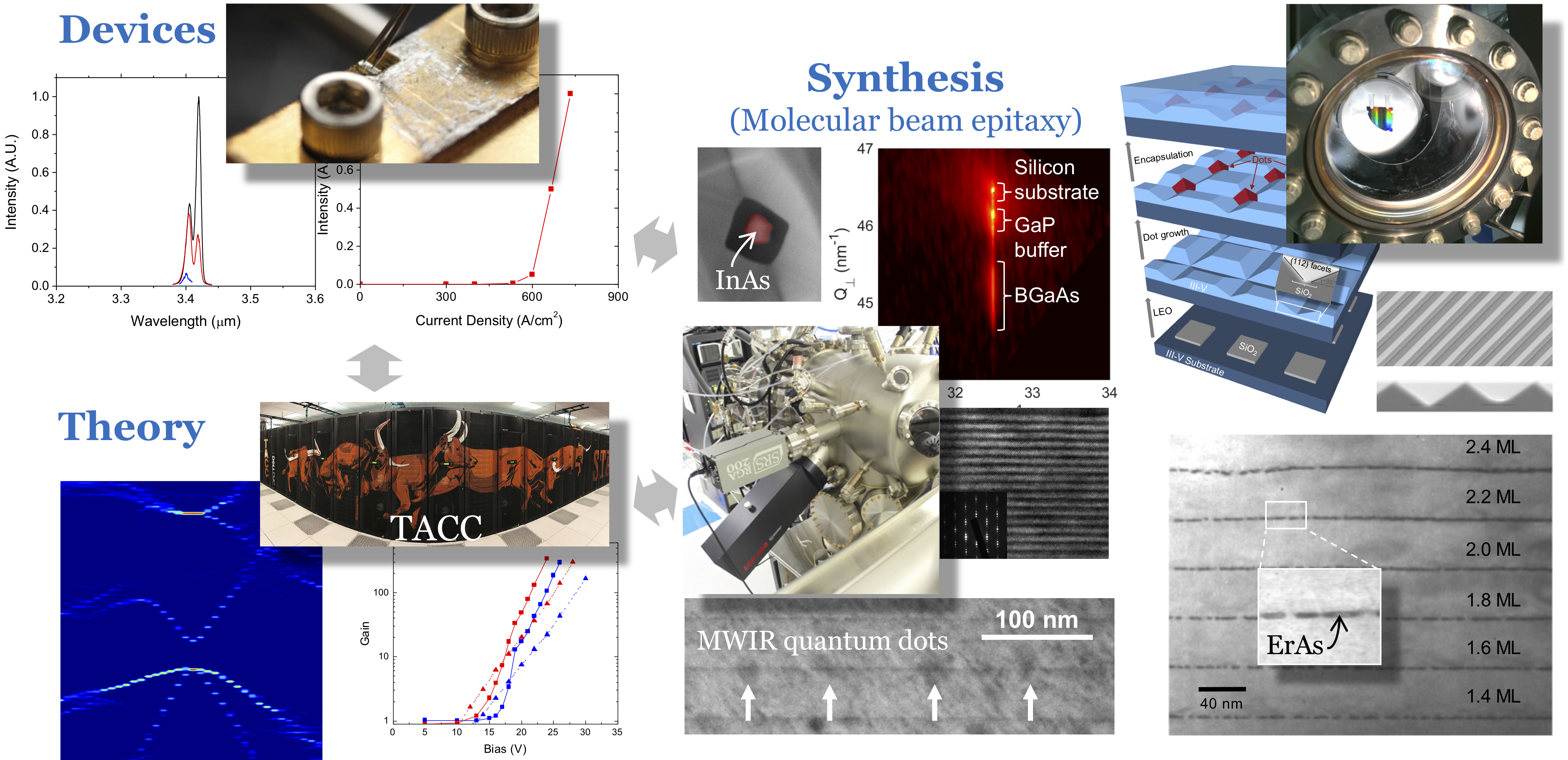
Compact, high-efficiency, mid-IR laser sources in the ~3-5 µm range are exciting for a number of applications including industrial gas monitoring, chemical/bio sensors, IR countermeasures, and communications systems. Current approaches to compact mid-IR sources include type-II “W” structures, quantum cascade lasers (QCLs), and type-I quantum wells on GaSb. Type-I GaInAsSb/AlGaAsSb active regions grown on GaSb offer significant advantages over other approaches, including room temperature operation, low threshold current density, high output power, and temperature stable operation. Specifically, they feature more straightforward device design and growth than QCLs and substantially higher gain and operating temperatures than W structures.
Low-noise III-V avalanche photodetectors
Avalanche photodetectors exhibit built-in gain and can operate at high bandwidths, making them critical in fiber-optic systems, 3-D laser radar (LIDAR), sensing systems, etc. We have demonstrated the highest gain, low noise, InAs avalanche photodetectors, the first working staircase avalanche photodetector, the first quaternary alloy exhibiting low excess noise, and the first low-noise III-V avalanche photodetector operating at the standard wavelength of fiber optic communications (1.55 μm).
Epitaxial metal-based nanophotonic materials and devices
We have been actively studying the introduction of plasmonic functionality into the heart of modern photonic devices, which necessitates plasmonic materials that can be epitaxially-integrated with III-V optically-active materials (e.g. quantum wells and dots). We have achieved record high plasma frequencies for InAs:Si, the first demonstration of plasmonic response from rare earth monopnictides (e.g. ErAs), the first demonstration of demonstration of compositional tuning of plasmonic properties (e.g. LaLuGdAs), and the first all-epitaxial plasmonic light emitting diodes (LED).
Integrated Photonics
We are actively working on ways to seamlessly integrate arbitrary patterned metals, dielectrics, and active semiconductors together epitaxially to enable radical new device structures and integrated photonic systems. In particular, we are working towards a photonic integrated circuit platform for quantum information processing.
Quantum information processing materials and devices
We are studying the doping of III-V materials with rare-earth elements as long-lived memory elements and quantum transducers, room temperature photon number resolving avalanche photodiodes, electrically-driven entangled photon sources, and photonic integration of active/passive quantum devices (sources, detectors, passives, etc.).
Metal/semiconductor nanocomposites for terahertz (THz) generation
There is currently a great need for systems to detect and identify chemical and biological agents. The 0.3-3 THz frequency range is a critical regime for such applications because of the many vibrational and rotational lines of key chemical/biological agents. The needs of such systems: high sensitivity/specificity, compact, rugged, portable, and power efficient place significant demands upon the THz sources. They must operate at room temperature and be widely tunable with narrow linewidth and high output power, electrically-driven, power-efficient, compact/rugged, and (preferably) operate cw. This requires sources that are far superior to those currently available. We are investigating new epitaxial metal/semiconductor nanocomposites to dramatically increase the performance of photomixer THz sources.
(Practical) silicon-based lasers
It has long been recognized that the integration of silicon-based electronics with photonics could be extremely powerful. This field has blossomed in recent years with the realization that on-chip interconnects are fast becoming a substantial source of power dissipation and delay. This coincides with historical progression of light as the preferred data transmitting medium on progressively smaller and smaller length scales: from ocean-to-ocean, city-to-city, ..., board-to-board, chip-to-chip, and eventually on-chip. Virtually all of the necessary optical components are in place for silicon-based optoelectronics, with the key exception being a monolithic, electrically-pumped, CMOS-compatible laser. The ultimate length scales and applications that optics will penetrate will depend on whether the silicon-laser problem can be solved, as well as its ultimate performance.
III-V transistors on silicon
The ITRS roadmap predicts serious difficulties in the coming years with simply scaling silicon CMOS. As a result, the silicon MOSFET is being virtually reinvented; high-k dielectrics are replacing SiO2 as the preferred oxide in MOSFETs. As a result, the arguments for a Si or SiGe channel become far less compelling. We are collaborating with Professors Sanjay Banerjee and Jack Lee to develop high-performance III-V MOSFETs.
Applying wireless communications approaches to optical fibers
In collaboration with Professor Sriram Vishwanath, we are studying the use of wireless signaling techniques (e.g. MIMO) to communications over conventional multimode optical fibers. Using these techniques, we have exceeded the bandwidth-length product of a conventional fiber by >15x, using only off-the-shelf-components.